2.6_GPU_Architecture
2.6 GPU Architecture
Three distinct GPU architectures can run CUDA.
Tesla hardware debuted in 2006, in the GeForce 8800 GTX (G80).
Fermi hardware debuted in 2010, in the GeForce GTX 480 (GF100).Kepler hardware debuted in 2012, in the GeForce GTX 680 (GK104).
The GF100/GK104 nomenclature refers to the ASIC that implements the GPU. The “K” and “F” in GK104 and GF100 refer to Kepler and Fermi, respectively.
The Tesla and Fermi families followed an NVIDIA tradition in which they would first ship the huge, high-end flagship chip that would win benchmarks. These chips were expensive because NVIDIA's manufacturing costs are closely related to the number of transistors (and thus the amount of die area) required to build the ASIC. The first large "win" chips would then be followed by smaller chips: half-size for the mid-range, quarter-size for the low end, and so on.
In a departure from that tradition, NVIDIA's first Kepler-class chip is targeted at the midrange; their "win" chip shipped months after the first Kepler-class chips became available. GK104 has 3.5B transistors, while GK110 has 7.1B transistors.
2.6.1 OVERVIEW
CUDA's simplified view of the GPU includes the following.
A host interface that connects the GPU to the PCI Express bus
0 to 2 copy engines
A DRAM interface that connects the GPU to its device memory
Some number of TPCs or GPCs (texture processing clusters or graphics processing clusters), each of which contains caches and some number of streaming multiprocessors (SMs)
The architectural papers cited at the end of this chapter give the full story on GPU functionality in CUDA-capable GPUs, including graphics-specific functionality like antialiased rendering support.
Host Interface
The host interface implements the functionality described in the previous section. It reads GPU commands (such as memcpy and kernel launch commands) and dispatches them to the appropriate hardware units, and it also implements the facilities for synchronization between the CPU and GPU, between different engines on the GPU, and between different GPUs. In CUDA, the host interface's functionality primarily is exposed via the Stream and Event APIs (see Chapter 6).
Copy Engine(s)
Copy engines can perform host device memory transfers while the SMs are doing computations. The earliest CUDA hardware did not have any copy engines; subsequent versions of the hardware included a copy engine that could transfer linear device memory (but not CUDA arrays), and the most recent CUDA hardware includes up to two copy engines that can convert between CUDA arrays and linear memory while saturating the PCI Express bus.
DRAM Interface
The GPU-wide DRAM interface, which supports bandwidths in excess of 100 GB/s, includes hardware to coalesce memory requests. More recent CUDA hardware has more sophisticated DRAM interfaces. The earliest (SM 1.x) hardware had onerous coalescing requirements, requiring addresses to be contiguous and 64-, 128-, or 256-byte aligned (depending on the operand size). Starting with SM 1.2 (the GT200 or GeForce GTX 280), addresses could be coalesced based on locality, regardless of address alignment. Fermi-class hardware (SM 2.0 and higher) has a write-through L2 cache that provides the benefits of the SM 1.2 coalescing hardware and additionally improves performance when data is reused.
TPCs and GPCs
TPCs and GPCs are units of hardware that exist between the full GPU and the streaming multiprocessors that perform CUDA computation. Tesla-class hardware groups the SMs in "TPCs" (texture processing clusters) that contain texturing hardware support (in particular, a texture cache) and two or three streaming multiprocessors, described below. Fermi-class hardware groups the SMs in "GPCs" (graphics processing clusters) that each contain a raster unit and four SMs.
For the most part, CUDA developers need not concern themselves with TPCs or GPCs because streaming multiprocessors are the most important unit of abstraction for computational hardware.
Contrasting Tesla and Fermi
The first generation of CUDA-capable GPUs was code-named Tesla, and the second, Fermi. These were confidential code names during development, but NVIDIA decided to use them as external product names to describe the first two generations of CUDA-capable GPU. To add to the confusion, NVIDIA chose the name "Tesla" to describe the server-class boards used to build compute clusters out of CUDA machines.[14] To distinguish between the expensive server-class Tesla boards and the architectural families, this book refers to the architectural families as "Tesla-class hardware," "Fermi-class hardware," and "Kepler-class hardware."
All of the differences between Tesla-class hardware and Fermi-class hardware also apply to Kepler.
Early Tesla-class hardware is subject to onerous performance penalties (up to 6x) when running code that performs uncoalesced memory transactions. Later implementations of Tesla-class hardware, starting with the GeForce GTX 280, decreased the penalty for uncoalesced transactions to about 2x. Tesla-class hardware also has performance counters that enable developers to measure how many memory transactions are uncoalesced.
Tesla-class hardware only included a 24-bit integer multiplier, so developers must use intrinsics such as __mul24() for best performance. Full 32-bit multiplication (i.e., the native operator * in CUDA) is emulated with a small instruction sequence.
Tesla-class hardware initialized shared memory to zero, while Fermi-class hardware leaves it uninitialized. For applications using the driver API, one subtle side effect of this behavior change is that applications that used cuParamSeti() to pass pointer parameters on 64-bit platforms do not work correctly on Fermi. Since parameters were passed in shared memory on Tesla class hardware, the uninitialized top half of the parameter would become the most significant 32 bits of the 64-bit pointer.
Double-precision support was introduced with SM 1.3 on the GT200, the second-generation "win" chip of the Tesla family.[15] At the time, the feature was considered speculative, so it was implemented in an area-efficient manner that could be added and subtracted from the hardware with whatever ratio of double-to-single performance NVIDIA desired (in the case of GT200, this ratio was 1:8). Fermi integrated double-precision support much more tightly and at higher performance.[16] Finally, for graphics applications, Tesla-class hardware was the first DirectX 10-capable hardware.
Fermi-class hardware is much more capable than Tesla-class hardware. It supports 64-bit addressing; it added L1 and L2 cache hardware; it added a full 32-bit integer multiply instruction and new instructions specifically to support the Scan primitive; it added surface load/store operations so CUDA kernels could read and write CUDA arrays without using the texture hardware; it was
the first family of GPUs to feature multiple copy engines; and it improved support for C++ code, such as virtual functions.
Fermi-class hardware does not include the performance counters needed to track uncoalesced memory transactions. Also, because it does not include a 24-bit multiplier, Fermi-class hardware may incur a small performance penalty when running code that uses the 24-bit multiplication intrinsics. On Fermi, using operator * for multiplication is the fast path.
For graphics applications, Fermi-class hardware can run DirectX 11. Table 2.1 summarizes the differences between Tesla- and Fermi-class hardware.
Texturing Niceties
A subtle difference between Tesla- and Fermi-class hardware is that on Tesla-class hardware, the instructions to perform texturing overwrite the input register vector with the output. On Fermi-class hardware, the input and output register vectors can be different. As a result, Tesla-class hardware may have extra instructions to move the texture coordinates into the input registers where they will be overwritten.
Table 2.1 Differences between Tesla- and Fermi-Class Hardware
Up to 2x for Tesla2 hardware.
"Up to 2x if ECC is enabled.
Another subtle difference between Tesla- and Fermi-class hardware is that when texturing from 1D CUDA arrays, Fermi-class hardware emulates this functionality using 2D textures with the second coordinate always set to 0.0. Since this emulation only costs an extra register and very few extra instructions, the difference will be noticed by very few applications.
2.6.2 STREAMING MULTIPPROCESSORS
The workhorse of the GPU is the streaming multiprocessor, or SM. As mentioned in the previous section, each TPC in SM 1.x hardware contains 2 or 3 SMs, and each GPC in SM 2.x hardware contains 4 SMs. The very first CUDA-capable GPU, the G80 or GeForce 8800 GTX, contained 8 TPCs; at 2 SMs per TPC, that is a total of 16 SMs. The next big CUDA-capable GPU, the GT200 or GeForce GTX 280, increased the number of SMs/TPC to 3 and contained 10 TPCs, for a total of 30 SMs.
The number of SMs in a CUDA GPU may range from 2 to several dozen, and each SM contains
Execution units to perform 32-bit integer and single- and double-precision floating-point arithmetic
Special function units (SFUs) to compute single-precision approximations of log/exp, sin/cos, and rcp/rsqrt
A warp scheduler to coordinate instruction dispatch to the execution units
A constant cache to broadcast data to the SMs
Shared memory for data interchange between threads
Dedicated hardware for texture mapping
Figure 2.29 shows a Tesla-class streaming multiprocessor (SM 1.x). It contains 8 streaming processors that support 32-bit integer and single-precision floating-point arithmetic. The first CUDA hardware did not support double precision at all, but starting with GT200, the SMs may include one double-precision floating-point unit.[17]
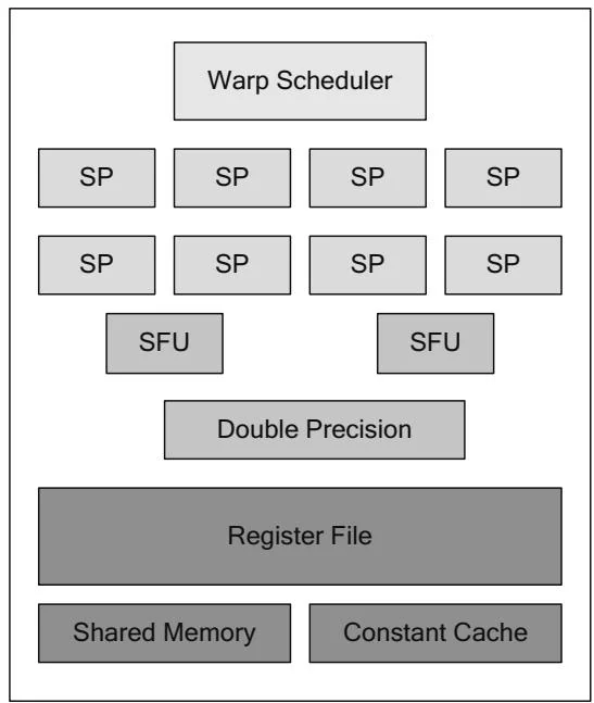
Figure 2.29 Streaming multiprocessor 1.x.
Figure 2.30 shows a Fermi-class streaming multiprocessor (SM 2.0). Unlike Tesla-class hardware, which implemented double-precision floating-point support separately, each Fermi-class SM has full double-precision support. The double-precision instructions execute slower than single precision, but since the ratio is more favorable than the 8:1 ratio of Tesla-class hardware, overall double-precision performance is much higher.[18]
Figure 2.31 shows an updated Fermi-class streaming multiprocessor (SM 2.1) that may be found in, for example, the GF104 chip. For higher performance, NVIDIA chose to increase the number of streaming processors per SM to 48. The SFU-to-SM ratio is increased from 1:8 to 1:6.
Figure 2.32 shows the most recent (as of this writing) streaming multiprocessor design, featured in the newest Kepler-class hardware from NVIDIA. This design is so different from previous generations that NVIDIA calls it "SMX" (next-generation SM). The number of cores is increased by a factor of 6 to 192,
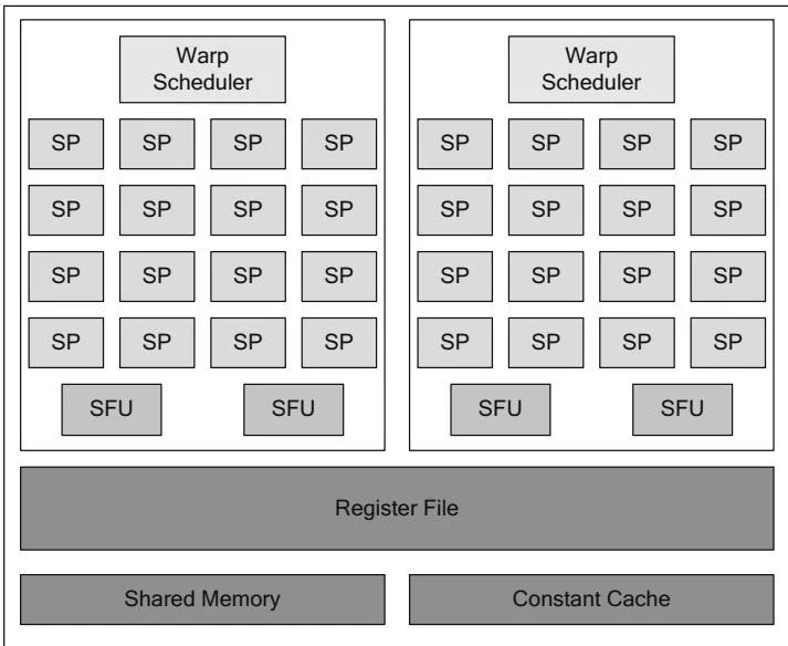
Figure 2.30 SM 2.0 (Fermi).
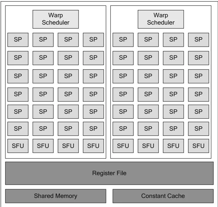
Figure 2.31 SM 2.1 (Fermi).
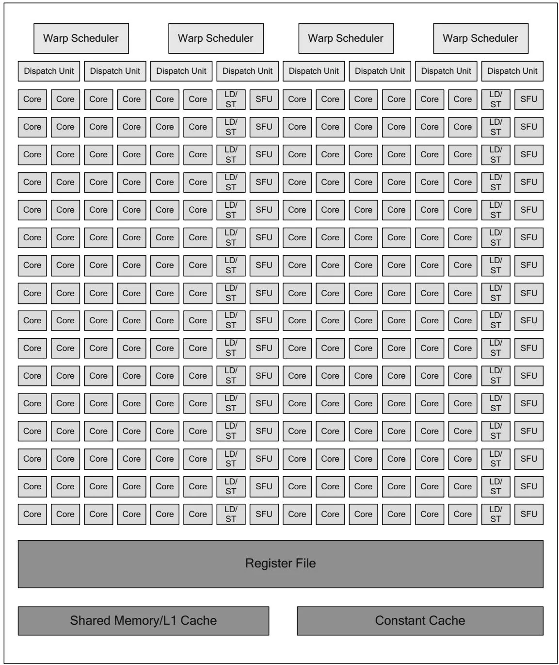
Figure 2.32 SM 3.0 (SMX).
and each SMX is much larger than analogous SMs in previous-generation GPUs. The largest Fermi GPU, GF110, had about 3 billion transistors containing 16 SMs; the GK104 has 3.5 billion transistors and much higher performance but only 8 SMX's. For area savings and power efficiency reasons, NVIDIA greatly increased the resources per SM, with the conspicuous exception of the shared memory/L1 cache. Like Fermi's SMs, each Kepler SMX has 64K of cache that can be partitioned as 48K L1/16K shared or 48K shared/16K L1. The main implication for CUDA developers is that on Kepler, developers have even more incentive to keep data in registers (as opposed to L1 cache or shared memory) than on previous architectures.